
When you first start out in the PCB layout game and know just enough to be dangerous, you simply plop down a connector, run a trace or two, and call it a hack. As you learn more about the finer points of inconveniencing electrons, dipping toes into the waters of higher performance, little details like via size, count, ground plane cutouts, and all that jazz start to matter, and it’s very easy to get yourself in quite a pickle trying to decide what is needed to just exceed the specifications (or worse, how to make it ‘the best.’) Connector terminations are one of those things that get overlooked until the MHz become GHz. Luckily for us, [Rob Ruark] is on hand to give us a leg-up on how to get decent performance from edge-launch SMA connections for RF applications. These principles should also hold up for high-speed digital connections, so it’s not just an analog game.
Everything that happens to those unfortunate electrons along their travels will affect performance in a subtle way, but the higher the frequency components of a signal, the worse it gets. An SMA edge connector may be designed to present a characteristic impedance of 50Ω typically, but that is to the end of the connection pins. Once it’s soldered down, there is a discontinuity unless precautions are taken. Even the transition from the pad to the signal trace can push a system out of spec, but what about the stack-up? What about the ground plane under the pad?
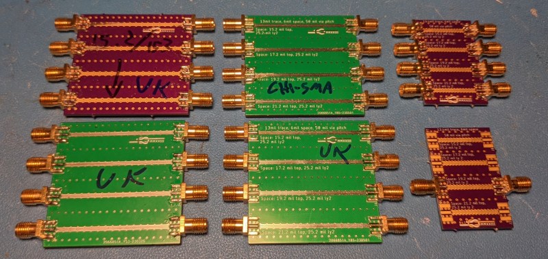
The first part of the job is to lock down your PCB process, via a specific stack-up. Every PCB house and line within it is different from the next, so it is critical to get hold of the layer arrangement, foil and dielectric thicknesses, dielectric constants, and loss tangent figures. [Rob] took a typical route, making a first stab at a footprint design supported by lots of online calculators (like these by Chemandy Electronics) and reference material. The basic structure is the usual coplanar waveguide, where the e-field is constrained by the ground plane below and leaks over the top of the trace. This resulted in a set of test coupons (small test PCBs) for two fab processes in parallel, OSHPark and JLCPCB.
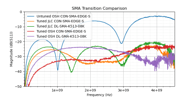
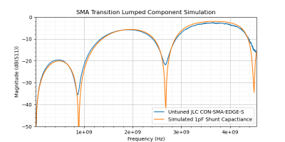
The returned PCBs were characterised using a NanoVNA V2 Plus, to get the S11 (return loss) curve up to about 4.5 GHz, confirming at about -26 dB they were already in a good position for optimisation. [Rob] also goes into some details about how to line up a QUCS simulation of a lumped transmission line model with the measured test coupon performance, which is well worth digging into.
PCB design is about functionality, but it is also about aesthetics and other factors that come out of that. Also on the subject of transmission lines, there are other kinds of transmission lines to read about.
SMA Connector Footprint Design for Open Source RF Projects
Source: Manila Flash Report


0 Comments