
When I saw this year’s Supercon Vectorscope badge, I decided that I had to build one for myself. Since I couldn’t attend in-person, I immediately got the PCBs and parts on order. Noting that the GitHub repository only had the KiCad PCB file and not the associated schematics and project file, I assumed this was because everyone was in a rush during the days leading up to Supercon weekend. I later learned, however, that there really wasn’t a KiCad project — the original design was done in Circuit Maker and the PCB was converted into KiCad. I thought, “how hard can this be?” and decided to try my hand at completing the KiCad project.
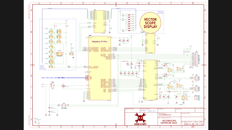
Fortunately I didn’t have to start from scratch. The PCB schematics were provided, although only as image files. They are nicely laid out and fortunately don’t suffer the scourge of many schematics these days — “visual net lists” that are neither good schematics nor useful net lists. To the contrary, these schematics, while having a slightly unorthodox top to bottom flow, are an example of good schematic design.
Graphical Lines to PCB Traces
The first thing I took a look at was the features on the PCB file, since I was hoping to extract the net names from the traces. Unfortuantely, when I looked at the traces, they were just graphical lines. I knew from previous digging on the KiCad user forums that going backwards from a PCB to a schematic is an unnatural workflow. But I was surprised that there in recent versions of KiCad ( I am using v7 ) there is a feature to convert graphical lines into traces.
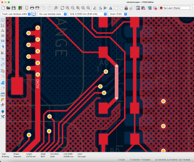
One non-obvious quirk to be aware of — this operation duplicates the selected the graphical lines before converting them into traces, resulting overlapping elements. This can be confusing, because the newly-created trace is presented by PCBNEW as being underneath the original graphical line, making it appear that the conversion failed. The solution is to immediately delete the selected items, and the converted tracks will remain. You can do this on an entire board at once by disabling everything except graphical items in the selection filter and just select an entire layer for conversion.
Part Footprints
When designing a PCB, the task of mapping the schematic symbols into their corresponding physical footprints can be tedious. Most modern CAD tools with their corresponding parts management schemes make this process easier than ever, but it can still be a headache when you are using parts not in the libraries. We’re going backwards in this design, so I wasn’t quite sure what problems might exist. But a quick glance at the PCB file shows that the parts on the board are really footprints. This seems promising, so let’s move on to making schematics.
Automatic Schematic Generation?
The usual design flow is from schematics to PCB, whether you’re using a CAD tool or doing everything by hand. Changes to a schematic are reflected on the PCB layout. Modern PCB CAD tools can update a PCB design automatically from the schematics, updating the net list and adding and/or removing parts as needed. These tools even take a stab at placing any new parts for you. Even if this is only a jumbled cluster of footprints, it’s easier than adding each part manually. But can you go the other direction?
There are also long-established processes for going the other direction, from PCB to the schematics, which have been around longer than computerized CAD tools. Perhaps the most common of these is called back annotation. Once the layout is substantially complete, the designer will re-sequence the reference designators on the board so that they appear in some order and are easy to find by people working on the PCB. We often skip this step for the kinds of small boards people make today, but if you’re making a 9U Eurocard design that is some 350 mm square, you really need to re-sequence the reference designators and back annotate the schematic.
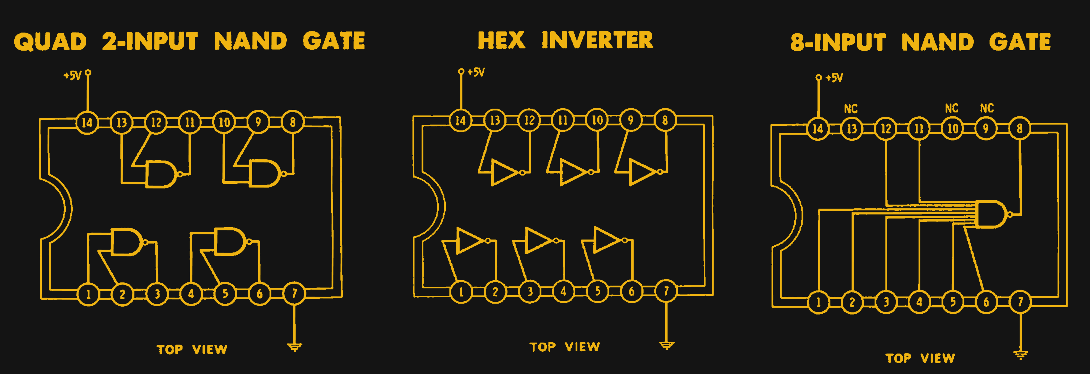
Another example of this backwards flow is gate swapping, so-named because it was very common in old designs using 74-series TTL logic chips. These chips have multiple gates per chip, single logic gates with multiple inputs, or both. Fortunately, CAD tools such as KiCad have provisions for these as well.
But we have the complete opposite of the normal “have a schematic and want to populate a new blank PCB” situation. Can I get KiCad to similarly populate a schematic from an existing PCB, no matter how ugly and disorganized it would be? Conceptually it doesn’t seem far fetched, given the existing KiCad capabilities. But in practice, the answer is no.
Make Schematics
Not unexpectedly, I needed to re-draw these schematics from scratch. Fortunately, this project doesn’t have a lot of parts and many of those parts are standard and found in KiCad or my own libraries. Equipped with the original documentation, I proceeded to draw the schematics in KiCad. Rather than making an exact duplicate of the existing schematics, I decided to rearrange the flow of the circuit into the more familiar left-to-right direction.
I started with just the main chips and components, ignoring connections and discrete components at first. Some of the parts weren’t in my libraries and had to be constructed in the KiCad symbol editor. I normally start with a large schematic sheet, realizing the page can always be resized later if needed ( I guessed A3, which turned out to be correct ). With all the chips on the page, you have to move things around until the visual flow on the page describes the actual logical flow of the design. Similar to placing components on a new PCB layout, there is no clear-cut process to place schematic symbols on a blank page. But here are some general concepts that I’ve learned over the years that I find helpful:
- Take a step back from circuitry, and consider the inputs, outputs, and functionality of the overall design as if it were a black box.
- Flow goes from left to right, inputs on left, outputs on right.
- Connectors go on the sheet edges, or for large designs, put all connectors on page 1.
- Group circuits together by function on the page, or for large designs, into hierarchical sheets.
- Avoid signal-name-only hidden connections (those without a wire) when possible — try to arrange the parts so all pins can be connected by wires.
- Use signal buses when applicable and when it helps the visual flow of the circuit.
There are many exceptions and contradictions within these guidelines. And the quality of the results can be subjective — give the same circuit, two different engineers could both preapre two different but good schematics.
Know Your Tools, Tweak Your Symbols
If you’ve ever sketched a circuit on paper, you usually make chips starting from an empty rectangle and then add signals where they are needed to make things flow. For many chips, like an 8-bit latch, the logical arrangement for your circuit matches up with the standard symbol diagrams provided by the manufacturer and/or your CAD tool libraries. But this is far from universal, especially when it comes to complex chips like microprocessors or FPGAs.
Don’t be afraid to tweak the schematic symbols to match your needs if necessary (being sure to use a local project-specific copy of the symbol). Remember the multiple-gates-per-IC feature of your EDA tool, like a hex inverter or a quad comparator package. This can be used to break up large chips into smaller manageable chunks. This is often used to separate the power supply pins of large chips into a separate symbols. But you can be further subdivide the chip into smaller symbols as needed by the overall signal flow of your design.
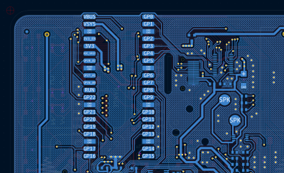
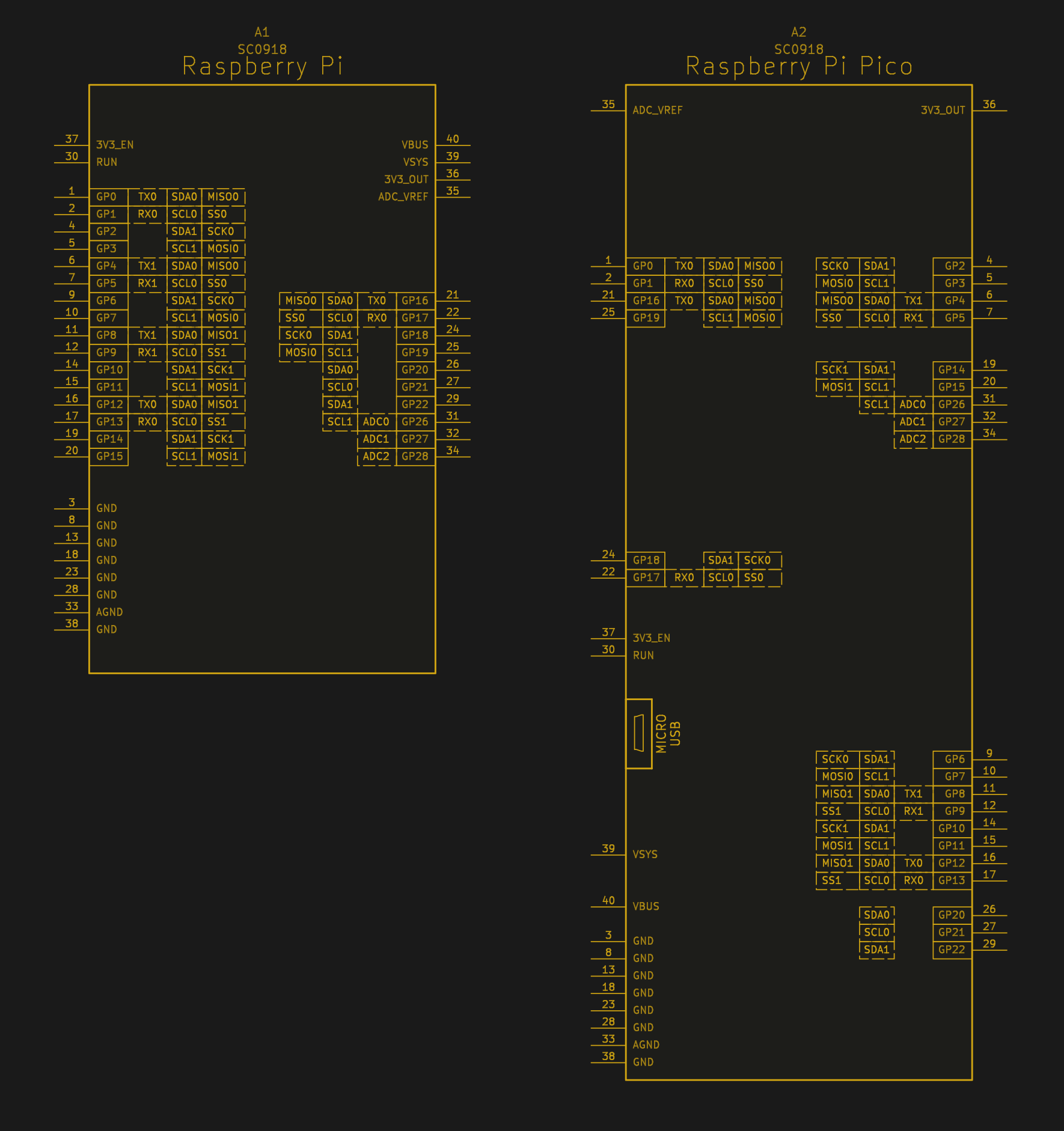
But probably the most helpful tweak is to simply rearrange the location of pins on the symbol and its size to better match your circuit. Consider the schematic symbol of a Raspberry Pi Pico module, which is arranged in a familiar pattern by GPIO number. Following that is the same Pico module after being tweaked to fit into the redrawn Vectorscope schematics.
Wrapup
There were a few issues between the original schematics and the PCB layout, but those have been sorted out. Some of the part footprints on the PCB are not footprints after all. Instead, they appear as a bunch of independent pads. And some parts have a discrepancy between the PCB pattern and the parts purchased from the BOM.
Just a few of the nets on the original schematic have names, and the rest are just blank. In the schematics, I tried to pick reasonable net names for the nets. I think this will be helpful when I eventually make the connection between the schematics the PCB.
At this point, I’ve completed what I wanted to in the beginning — make a KiCad schematic for the Vectorscope project. The KiCad project is not 100% consistent, but I have dug into the few missing pieces and solving those issues is not going to be a huge effort. These issues are explained in the readme of the project’s GitHub repository.
Vectorscope KiCad Redrawing Project
Source: Manila Flash Report


0 Comments